433 MHz Power Amplifier 2W433 MHz Power Amplifier 2W BLT53A
This project explain how you can build your own RF Amplifier.
I will explain how to read datasheet and match the input and output networks.
I will make try to make it simple to follow and to understand
This is an educational project and you have to follow your local regulations when it comes to transmitter and power levels.
Background
I needed a good RF Amplifier for the 70 cm frequency band.
I found several units to buy on comercial places, but no one of them had good standard. They were cheap and so was the quality as well.
Is it that difficult to build an amplifier with good efficiency and good input/output impedance matching?
I wanted to build my own unit and fully understand how to design all parts.
I found a good transistor BLT53A which can deliver 3W at 6V drive according to datasheet.
The first thing is to understand the basic of an amplifier. Below I will explain it in details.
Hardware and schematic Transistors Input and Output impedances
The picture below show the basic of a transistor amplifier.
I will explain with the picture below. To the left is some kind of RF source signal. This is the rf-signal you want to boost up.
The signal is going into the blue box which is an impedance mathning filter. The rf signal then enter the yellow box which is the transistor.
The transistor gains the signal and it goes into the green box whis is again an impedance matching filter.
Finally there is some kind of load (or antenna).
Let's talk about the transistor. A transistor has a low input impedance at its Base. The same comes with the output impedance at the Collector.
We have to consider this because if we don't do that, we will loose lot of power and gain in the amplifier. We will also have difficulty to drive an antenna.
How do we solve all this? The solution is to make a networks that convert a 50 Ohm system to match the transistors low impedances.
Look again at the picture. To the left you will find a RF source. This is the RF signal we want to boost up. This source is most often built to match 50 Ohm resistive load.
The blue box is an input matching network. It will transform its input (Zin Purple) to match the transistors impedance (Zin Blue)
If our input matching network is correct constructed, the RF source will
see 50 Ohm pure resistive impedance, and all the ennergy from the RF source will now be transferred into the transistor. Great!
(This is often named as having good SWR)
The same procedure is done at the output of the transistor. Our Load (Antenna) is most often 50 ohm resistive part. So the output matching network should convert the
output impedance of the transistor (Zout Green) to pure 50 Ohm resisitve (Zout Purple).
If our output matching network is correct constructed, the output energy of the transistor will be transferred to the load which is a 50 Ohm resistive part.
All the ennergy will now end up in our 50 Ohm load (antenna). Great again!
So the first thing we need to do is to find information about our transistor BLT53A.
Finding the input and output impedances of transistor BLT53A
Below you will find a table with lot of information about the transistor.
Sometimes manufacturer give this information in the datasheet, and sometimes it can be difficult to find it.
I was lucky to find this information and I will explain what we see here and how to use it.
To the left is the frequency and it start at 0.1GHz = 100 MHz. Then comes S11, S21, S12, and S22.
I will not go into details about the S-parameters because it is a chapter of itself. If you wish to know details you can read this great pdf. Basic of S-parameters.pdf
Lets focus on S11 and the green square box which is the reflected power. S11 can be used to calculate the input impedance of the transistor.
Here we find that S11 in Polar form and it say MAG = 0.849 and ANG = 179.5
Let's conver that into Rectangular form at this homepage : convert-polar-rectangular
Below you can see the result, which gives -0.85 + 0.01j
We will need to make one more conversion from S-parameters to Z-parameters, before we get the input impedance.
Let's conver S parameters to Z parameters at this homepage : S-Y-Z-Parameter-Converter-Calculator
We now have the input impedance in complex format. It is 4.05 Ohm with a small imaginary part of 0.292 (Since the imaginary part is positive it means the input impedance has a small serial inductance)
Input matching network
As we found out the input impedance of the transistor was very low (4.05+j0.292).
We must now convert this to 50 Ohm using some kind of LC-network.
The picture below shows a schematic of a network which transform the 50 Ohm input impedance (R2) to a low transistor impedance (R1).
To the left is the common formula to calculate values of impedance matching filter. I will go around this and use excel to iterate different components values to find the match.
Excel calculation and iteration
Excel i very simple to use for calculating and plotting.
I will try to explain the calculation below in a simple way.
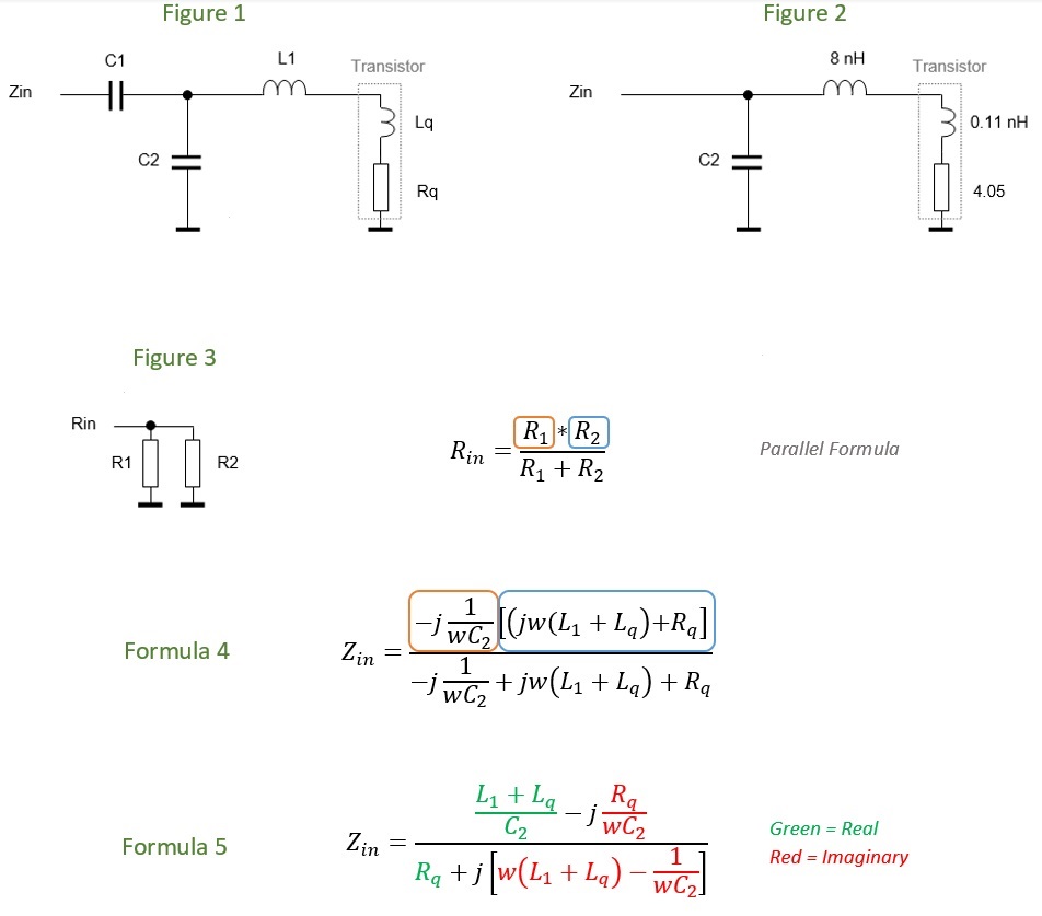
See below, figure 1 will show the input matching filter C1, C2, L1 and the Transistor. From datasheet we found the transistor to be Rq=4.05 and Lq=0.292 (since Lq is positive it means it is inductive)
The first thing we want to find the value of C2 to give 50 Ohm Resistive part of Zin. C1 will not contribute ANYTHING with Resistive part of Zin, so we will not focuse on that component for now.
In figure 2 I have removed C1 and I have given L1 a value of 8nH. Reactive part of Lq was positive and 0.292 so that means inductor of 0.11nH at 433MHz. (XL = wLq => 2*pi*f*Lq). Rq = 4.05.
Alright, figure 3 show a basic parallel connection between two resistors and the formula to calculate the Rin.
In figure 2 we can find C2 which is pralallel with the total inductance and the resistance of the transistor, so if we use the parallel formula we will get formula 4.
In formula 4 you can identify R1=orange color and R2=blue color but in complex form.
After cleaning up formula4 we get formula 5. Here we have a division of two complex numbers giving Zin.
Let's take a look at formula 5. First I have green for the Real part and Red for Imaginary part.
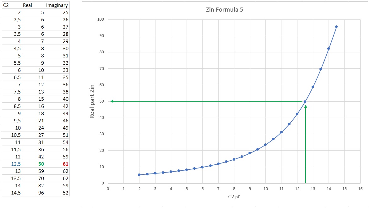
The only variable we do not know is C2. I will put the formula into excel and I will iterate C2 from 2 pF to 14.5 pF and find out What Zin will become.
The picture below will show you the plot of Zin when C2 go from 2 to 14.5 pF.
In the table to the left you will see the value of C2 and the complex value of Zin.When C2 is 12.5pF we will see that th Real part of Zin is equal to 50 ohm. Perfect!
You may now wonder what about the red +61 Imaginary parth then?
I will show how to remove that part in next section.
Removing the Imaginary part of Zin
From the Formula 5 we found the we had a imaginary part of +61. Since it is positive it means it is inductive in nature.
How do we remove that part?
It is easy, since C1 in Figure 1 is capacitive (oposite) it will be used to cancel out the imaginary part from Zin.
So which vale of C1 will give -61 at 433 MHz.
The formula for capacitive reactance is 1/wC (w= 2*pi*f)
so, 61 = 1/(2*pi*433e6*C1) gives C1 = 6 pF
When C1 is 6 pF it will add -j61 imaginary part to the Zin which will cancel out the +j61 and we have only 50 ohm pure resistive impedance left.
By choosing C1 = 6pF and C2 = 12.5pF and L = 8 nH we will have 50 Ohm resistive input of the filter and all energy will be transformed to match the input impedance of the transistor
Output matching network
The output matching networks is calculated exactly the same way. I will not show all screendumps to calculate it, just give the values.
Lets focus on S22 and the red square box which is the reflected power in the datasheet. S22 can be used to calculate the output impedance of the transistor.
Here we find that S22 in Polar form and it say MAG = 0.852 and ANG = 174.5
Let's conver that into Rectangular form and we get: -0.85 + 0.08j
We convert S parameters to Z parameters and the output impedance in complex form is : 3.95 + 2.33j
We now have the output impedance in complex format. It is 3.95 Ohm with a imaginary part of 2.33j (Since the imaginary part is positive it means the input impedance has a small serial inductance)
The picture below is a similar excel iteration to find C2.
We have 50 ohm resistance when C2 is about 11.4pF
Lets fix C2 to 11.4pF and we will make a new iteration only changing C1.
Lets look at the plot below and I will explain what we see there.
The Y-axel above will now show the reactance. We wish it to be zero because we do not want any load from capacitance or inductance at R2.
We will find that the reactance is zero when C1 is 5.2 pF ...Great!
By choosing C1 = 5.2pF and C2 = 11.4pF and L = 8 nH we will have 50 Ohm resistive output of the filter and all energy from the transistor will be transferred to the antenna (load).
How about Gain?
Let's dig into the datasheet again.
The datasheet claim it can give +18dB gain. So if we want to have +33 dBm (2W) out, we need to feed it with 33-18 = +15dBm (32mW).
Schematic
Below you will find the schematic of this amplifier. Two resistors connected to the base of the transistor will bias the collector current.
To make the driving of this amplifier more easy, I added a simple MMIC. The MMIC will gain the input signal with 15-20dB to drive the amplifier transistor. The good thing with the MMIC is that is matched to 50 ohm at input and output.
By using a MMIC as pre-driver, I only need 0dBm (1mW) driving power to get +33dBm (2W) output.
Below you can see my experimental board. The unit has about 65% efficiency and the PCB is not getting very warm as many amplifiers often do.
Performance
Before we go into measurements and details, I want to share a link where you can convert reflection (return loss),SWR and reflection power in %. https://www.everythingrf.com/tech-resources/vswr
First let's have a look at the input matching. The picture below show the input match at 0dBm driving power.
The marker is at 434MHz and it show a SWR of 1.029, which means perfect 50 input match. No incoming energy reflects back.
You can find the SWR to the left on the scale. To give you a hint about SWR values : When SWR is 1.2 (yellow arrows) you will only loose 1% of your energy in reflections, which is nothing...
What more do we see, well the frequency span in this measurement is 50 MHz, so each frame is 5 MHz whide. This means we have a very good match several MHz around 434 MHz.
The screenshot to the right shows the gain. We feed this unit with 0 dBm and at 434 MHz we have +33 dBm.
Let's look at the output signal in a spectrum analyser.
The signal is attenuated externally with 33dB and internally with 10dB, so totally 43dB. The spectrum analyser show a nice peak referring to +33dBm (2W) power and with no distortion of the signal.
The second screenshot will show a wider frequency span (up to 1.5GHz). Here we can see all 3 peaks, fundamental and the 2 overtones.
The good thing here is that the overtones are well below the fundamental (30dB) as they should be. Remember this amplifier has not much filtering added. You can of course add lowpass filter at the output to attenuate the overtones.
Pre Amplifier
Some has asked me how I drive the final transistor. On my experimental board I use a simple MMIC. it delivers about +15.8 dBm, which is enough.
Below you can see both reflection and amplification of the MMIC amplifier. The highlighted Meas1:Mkr1 in the picture show the reflection which is -30.410 dB.
This is a very good match and it is equal to a reflection of 0.1% of incomming energy (SWR=1.06)
When final transistor was added and some new tuning I had even better SWR=1.03 (see measurement above)
The other Meas2:Mkr1 show you the gain which is 15.8 dB (+15.8dBm)
Temperature
I have run the Amplifier continuously without any heatzink and in open air-space the PCB become +50 Celsius, which is no problem for the unit.
Final word
I hope you have enjoyed reading about this rf project.
Hopefully you have found new inspiration for your own projects. I will ofcourse share your projects here if you wish.

 433 MHz Power Amplifier 2W